Printed Circuit Boards (PCBs) are integral to modern electronics, and their reliability is paramount. When failures occur, it is crucial to identify the root causes to improve design, manufacturing processes, and overall product reliability. Here’s a comprehensive overview of some of the most important PCB failure analysis techniques in practice today.
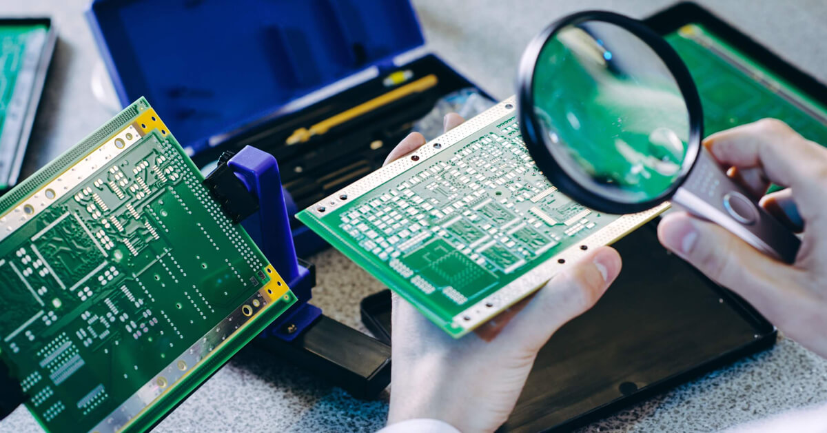
1. Visual Inspection
Visual inspection is often the first step in PCB failure analysis. It involves examining the PCB with the naked eye or using magnification tools like stereo microscopes and metallographic microscopes. This method helps identify obvious defects such as cracks, corrosion, discoloration, and physical damage. Visual inspection is essential for locating failure sites and understanding the failure mode.
2. X-ray Fluoroscopy
X-ray fluoroscopy is used to inspect internal structures and hidden defects that are not visible through visual inspection. This technique is particularly useful for examining solder joints, through-holes, and high-density interconnects (HDIs). X-ray systems can detect voids, cracks, and misalignments within the PCB layers and components. Advanced systems offer three-dimensional imaging, providing detailed insights into the internal condition of the PCB.
3. Cross-Sectional Analysis (Microsectioning)
Cross-sectional analysis, also known as microsectioning, involves cutting a small section of the PCB to examine its internal structure under a microscope. This technique provides valuable information about the quality of solder joints, plating, and the integrity of vias and traces. The process includes embedding the sample in epoxy, polishing it to a smooth finish, and then etching it to reveal the internal features. Microsectioning is crucial for understanding the root causes of failures related to manufacturing defects and material inconsistencies.
4. Scanning Electron Microscopy (SEM)
Scanning Electron Microscopy (SEM) offers high-resolution imaging of the PCB surface and cross-sections. SEM can magnify features up to 100,000 times, allowing for detailed examination of microstructural defects, contamination, and surface morphology. Additionally, SEM can be combined with Energy Dispersive X-ray Spectroscopy (EDS) to analyze the elemental composition of materials, helping identify contamination and material defects.
5. Thermal Imaging
Thermal imaging, or infrared thermography, is used to detect thermal anomalies on the PCB. This technique involves capturing infrared images of the PCB while it is powered and operational. Thermal imaging can identify hotspots, which may indicate issues such as short circuits, excessive current flow, or poor thermal management. By pinpointing areas of abnormal heat generation, engineers can diagnose and address potential failure points.
6. Electrical Testing
Electrical testing involves measuring the electrical properties of the PCB to identify faults. Techniques such as Time Domain Reflectometry (TDR) and Flying Probe Testing (FPT) are commonly used. TDR measures the impedance of traces and can detect discontinuities, while FPT uses probes to test the electrical connectivity of components and traces. Electrical testing helps identify open circuits, short circuits, and impedance mismatches.
7. Fourier Transform Infrared Spectroscopy (FTIR)
Fourier Transform Infrared Spectroscopy (FTIR) is used to analyze the chemical composition of materials on the PCB. FTIR can identify organic contaminants, residues, and degradation products by measuring the absorption of infrared light at different wavelengths. This technique is valuable for identifying contamination sources and understanding the chemical changes that may have contributed to the failure.
8. Ion Chromatography
Ion chromatography is a technique used to detect and quantify ionic contaminants on the PCB. Ionic contaminants, such as chlorides and sulfates, can lead to corrosion and electrical leakage. Ion chromatography involves extracting ions from the PCB surface and analyzing them using a chromatograph. This method helps identify contamination sources and assess the effectiveness of cleaning processes.
9. Acoustic Microscopy
Acoustic microscopy, or Scanning Acoustic Microscopy (SAM), uses high-frequency sound waves to inspect the internal structure of the PCB. This technique is particularly effective for detecting delaminations, voids, and cracks within the PCB layers and components. Acoustic microscopy provides a non-destructive means of examining the integrity of the PCB without the need for cross-sectioning.
10. Environmental Testing
Environmental testing involves subjecting the PCB to various environmental conditions to assess its reliability and durability. Tests may include thermal cycling, humidity exposure, vibration, and mechanical shock. By simulating real-world conditions, environmental testing helps identify potential failure modes and ensures that the PCB can withstand the intended operating environment.
Conclusion
PCB failure analysis is a multifaceted process that employs a variety of techniques to identify and understand the root causes of failures. From visual inspection and X-ray fluoroscopy to advanced methods like SEM and FTIR, each technique provides unique insights into the condition and performance of the PCB. By leveraging these techniques, manufacturers can improve the quality and reliability of their products, ensuring that they meet the stringent demands of modern electronics.