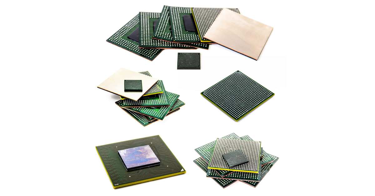
Designing compact printed circuit boards (PCBs) is a complex task that requires careful consideration of various factors to ensure functionality, reliability, and manufacturability. Here are the most important factors to consider when designing compact PCBs:
1. Component Placement and Orientation
Importance: Proper component placement is crucial for optimizing space and ensuring efficient routing. Incorrect placement can lead to longer trace lengths, increased signal interference, and difficulty in assembly.
Best Practices:
- Group Related Components: Place components that interact closely together to minimize trace lengths and reduce signal interference.
- Consider Heat Dissipation: Position heat-generating components away from sensitive areas and provide adequate spacing for heat sinks or thermal vias.
- Optimize Orientation: Align components in a way that facilitates efficient routing and minimizes the number of vias required.
2. Layer Stack-Up
Importance: The layer stack-up determines the overall thickness of the PCB and affects signal integrity, power distribution, and thermal management.
Best Practices:
- Use Multilayer PCBs: Employ multiple layers to separate power, ground, and signal traces, which helps in reducing electromagnetic interference (EMI) and improving signal integrity.
- Optimize Layer Order: Place power and ground planes close to signal layers to provide effective shielding and reduce noise.
- Consider HDI Technology: High-Density Interconnect (HDI) technology allows for more layers and finer traces, enabling more compact designs.
3. Trace Routing
Importance: Efficient trace routing is essential for maintaining signal integrity and minimizing crosstalk and EMI.
Best Practices:
- Keep Traces Short and Direct: Shorter traces reduce resistance and inductance, improving signal quality.
- Use Differential Pair Routing: For high-speed signals, use differential pairs to reduce noise and crosstalk.
- Avoid Sharp Angles: Use smooth curves or 45-degree angles instead of 90-degree bends to minimize signal reflection and impedance discontinuities.
4. Signal Integrity
Importance: Maintaining signal integrity is critical for the performance of high-speed and high-frequency circuits.
Best Practices:
- Control Impedance: Design traces with controlled impedance to match the characteristic impedance of the signal, reducing reflections and signal loss.
- Minimize Crosstalk: Increase spacing between high-speed traces and use ground planes to shield signals.
- Use Termination Techniques: Implement proper termination techniques, such as series or parallel termination, to prevent signal reflections.
5. Power Distribution Network (PDN)
Importance: A well-designed PDN ensures stable power delivery to all components, reducing noise and improving overall performance.
Best Practices:
- Use Power Planes: Employ dedicated power planes to provide low-impedance paths for power distribution.
- Decouple Capacitors: Place decoupling capacitors close to power pins of ICs to filter out noise and stabilize voltage levels.
- Optimize Via Placement: Use multiple vias to connect power planes and reduce impedance.
6. Thermal Management
Importance: Effective thermal management prevents overheating, which can damage components and reduce the lifespan of the PCB.
Best Practices:
- Use Thermal Vias: Implement thermal vias to transfer heat from hot components to other layers or heat sinks.
- Provide Adequate Spacing: Ensure sufficient spacing between heat-generating components and other parts to allow for proper airflow.
- Use Heat Sinks and Thermal Pads: Attach heat sinks or thermal pads to high-power components to dissipate heat efficiently.
7. Manufacturability
Importance: Designing for manufacturability ensures that the PCB can be produced reliably and cost-effectively.
Best Practices:
- Follow Design Rules: Adhere to the design rules provided by the PCB manufacturer, including minimum trace width, spacing, and via sizes.
- Panelization: Design the PCB layout to facilitate panelization, which improves manufacturing efficiency and reduces costs.
- Test Points: Include test points for easy testing and debugging during the manufacturing process.
8. Mechanical Constraints
Importance: Mechanical constraints, such as the size and shape of the PCB, must be considered to ensure it fits within the intended enclosure.
Best Practices:
- Define Board Outline: Clearly define the board outline and ensure it fits within the mechanical constraints of the final product.
- Consider Mounting Holes: Include mounting holes and ensure they are placed in locations that provide structural support and ease of assembly.
- Account for Connectors: Ensure that connectors are placed in accessible locations and do not interfere with other components or the enclosure.
9. Environmental Considerations
Importance: Environmental factors, such as temperature, humidity, and exposure to chemicals, can affect the performance and reliability of the PCB.
Best Practices:
- Select Appropriate Materials: Choose materials that can withstand the environmental conditions the PCB will be exposed to.
- Conformal Coating: Apply conformal coating to protect the PCB from moisture, dust, and chemicals.
- Temperature Ratings: Ensure that components and materials have appropriate temperature ratings for the intended operating environment.
10. Compliance with Standards
Importance: Compliance with industry standards ensures that the PCB meets safety, reliability, and performance requirements.
Best Practices:
- Follow IPC Standards: Adhere to IPC standards for PCB design, manufacturing, and assembly to ensure high quality and reliability.
- Regulatory Compliance: Ensure that the PCB design complies with relevant regulatory requirements, such as RoHS and REACH, to avoid legal and environmental issues.
- EMC Compliance: Design the PCB to meet electromagnetic compatibility (EMC) standards to prevent interference with other electronic devices.
Conclusion
Designing compact PCBs requires careful consideration of various factors to ensure functionality, reliability, and manufacturability. By focusing on component placement, layer stack-up, trace routing, signal integrity, power distribution, thermal management, manufacturability, mechanical constraints, environmental considerations, and compliance with standards, designers can create high-quality, reliable, and efficient compact PCBs. These best practices help overcome the challenges associated with miniaturization and ensure that the final product meets the demands of modern electronic applications.


