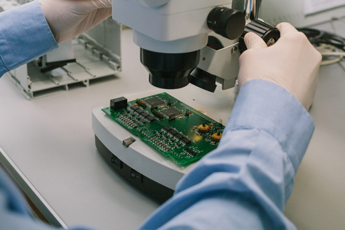
Printed Circuit Board (PCB) manufacturing techniques have evolved significantly over the years, with advancements in technology leading to more efficient and cost-effective processes. PCBs are an essential component of modern electronics, providing a platform for the interconnection of electronic components. In this essay, we will provide an overview of the various PCB manufacturing techniques.

The first step in PCB manufacturing is designing the circuit board layout using computer-aided design (CAD) software. The layout is then printed onto a copper-clad laminate sheet using a laser printer or photocopier. The next step is to etch away the unwanted copper using a chemical solution, leaving behind the desired copper traces that form the circuitry.
Another popular PCB manufacturing technique is the use of milling machines to create the circuit board. In this process, a CNC milling machine is used to remove unwanted copper from a blank copper-clad laminate sheet, leaving behind the desired circuitry. This technique is often used for creating complex PCBs with intricate designs.
Yet another technique used in PCB manufacturing is called "additive manufacturing." This technique involves depositing metal onto a substrate using inkjet printing or other similar methods. The metal is then selectively removed to create the desired circuitry. This technique is still in its early stages but has shown promise for creating high-density interconnects and other complex circuitry.
PCB manufacturing also involves drilling holes into the board for mounting components and providing electrical connections between layers. This process can be done using mechanical drills or laser drills, depending on the requirements of the project.
After drilling, the board undergoes a process called "through-hole plating," where metal is deposited inside the drilled holes to provide electrical connections between layers. The board is then coated with a layer of solder mask to protect it from oxidation and prevent short circuits.
Finally, the board undergoes a process called "surface finishing," which involves applying a layer of metal to protect the copper traces and provide a surface for soldering components. The most common surface finishes used in PCB manufacturing are HASL (hot air solder leveling), ENIG (electroless nickel immersion gold), and OSP (organic solderability preservatives).
In conclusion, PCB manufacturing techniques have come a long way since their inception, with advancements in technology leading to more efficient and cost-effective processes. From etching to milling to additive manufacturing, each technique has its own advantages and disadvantages. The choice of technique depends on the requirements of the project and the desired outcome.
For all your electronic assembly needs, please send us your project requirements now, either through our online quote tool, or to orders@optimatech.net. We strive to produce the highest quality PCBs and assemblies to meet all our customer needs.